


 English
TURN-KEY PCB ASSEMBLY: BITTELE ELECTRONICS
PCB MANUFACTURING AND ASSEMBLY
Full Turn-Key PCB Manufacturer
You can quickly get quotes and order PCB fabrication and assembly using our online system. Take advantage of exclusive automatic discounts with our tool. Our BOM pricing tool ensures you receive the lowest price for your order.
START A TURN-KEY PCB ORDER
Factors to Consider in Routing for High-Speed Signals in PCB Design
Routing high-speed signals on a PCB requires meticulous planning to ensure signal integrity and minimize issues like crosstalk, reflections, and electromagnetic interference (EMI).
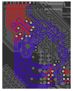
One of the primary considerations is impedance matching, which involves ensuring that the impedance of the signal traces matches the impedance of the source and load to minimize reflections and signal loss. Using controlled impedance traces, especially for differential pairs, is crucial. Additionally, trace length matching is essential for maintaining phase consistency and reducing skew, particularly for differential signals and other critical high-speed signals.
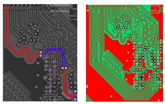
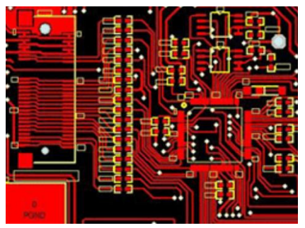
To minimize crosstalk, it's important to maintain adequate spacing between high-speed signal traces and use ground planes to provide a return path for signals and shield them from each other. The PCB layer stackup should be designed to provide a clear return path for high-speed signals, with signal layers placed adjacent to ground planes and isolated from power planes to reduce noise coupling. Via management is another critical aspect; reducing the number of vias in high-speed signal paths and using backdrilling to remove unused via stubs can help avoid signal degradation.

Proper termination techniques, such as series, parallel, or AC termination, should be used to match impedance and reduce reflections, with termination resistors placed close to the source or load as required. Ensuring power integrity involves placing decoupling capacitors close to high-speed ICs and using solid power planes for low impedance paths. Signal routing should follow the shortest and most direct path possible, avoiding 90-degree bends and using 45-degree bends or rounded corners to reduce signal reflections and impedance discontinuities.
For differential pair routing, maintaining equal lengths and consistent spacing between the pairs is essential for proper coupling and impedance control. Electromagnetic compatibility (EMC) can be achieved through shielding techniques to protect high-speed signals from external EMI and implementing good grounding practices.
By considering these factors, you can effectively route high-speed signals on your PCB and ensure reliable performance.
If you are interested in getting more detailed information about Bittele’s specific capabilities, we recommend you read our comprehensive High Speed PCB Design For Manufacturability (DFM) and PCB Design For Assembly (DFA) Guidelines documents. For more information about our capabilities with regard to high speed PCBs, or to send us your PCB Design Files for an official quotation, please feel free to Contact Us any time! We can be reached via email at sales@7pcb.com or call at 1-416-800-7540.
Please briefly describe the information you are seeking in the search bar below.