


 English
TURN-KEY PCB ASSEMBLY: BITTELE ELECTRONICS
PCB MANUFACTURING AND ASSEMBLY
Full Turn-Key PCB Manufacturer
You can quickly get quotes and order PCB fabrication and assembly using our online system. Take advantage of exclusive automatic discounts with our tool. Our BOM pricing tool ensures you receive the lowest price for your order.
START A TURN-KEY PCB ORDER
How to Prevent Solder Joint Voiding and Cold Solder Defects
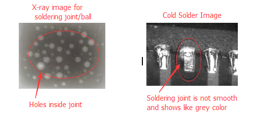
Solder joint voiding is a phenomenon that causes empty spaces or voids to occur within the joint. Solder joint voiding often occurs on BGAs and larger pads. Voids are related to flux that’s entrapped in the joint, as well as paste oxidation. A large number of voids will reduce the soldering joint’s reliability.
Analysis of Root Causes
- Too much flux is applied in the solder paste. The flux doesn’t have sufficient time to outgas before the solder has transitioned to a solid state.
- The preheat temperature is too low so any solvent in the flux is difficult to vapour out completely.
- The soak zone time is too short during the reflow process.
- Lead-free solder typically has a 4% shirinkage in volume when it is cooled down to a solid state. It is possible to obtain voids when large pads are cooled down unevenly.
- Paste oxidation occurs.
Corrective Actions
- Reduce the amount of solder paste deposited.
- For large pads, use small opening grids instead of a large aperture.
- Extend the preheat time so it is long enough.
- Extend the soak zone time so it is long enough.
- Always consider new solder paste for BGA assembly.
While a normal solder joint is usually bright and shiny, a cold Solder joint is an abnormally dull, non-reflective, rough surface on the solder joint.
Analysis of Root Causes
- The pre-heat time is too long and too high, preventing the flux from activating.
- The solder paste has expired.
- There is not enough heat absorbed by the solder.
- The cooling speed is too slow.
Corrective Action
- Adjust the reflow profile according to the manufacturer’s specification.
- Ensure the peak temperature is at least 15°C above the solder’s melting point for more than 45 seconds.
- Change to a new type of solder paste.
Related Articles:
- Which Soldering Defects are Related to the Incorrect Setup of the Reflow Profile?
- How to Prevent Solder Ball and Bridging Defects during the SMT Reflow Process
- How to Prevent the Tombstone and Open Defects during the SMT Reflow Process
- How to Prevent Solder Bridging in 3528 PLCC6 RGB LEDs?
- An Analysis of SMT Solder Paste Printing Defects
Please briefly describe the information you are seeking in the search bar below.