


 English
TURN-KEY PCB ASSEMBLY: BITTELE ELECTRONICS
PCB MANUFACTURING AND ASSEMBLY
Full Turn-Key PCB Manufacturer
You can quickly get quotes and order PCB fabrication and assembly using our online system. Take advantage of exclusive automatic discounts with our tool. Our BOM pricing tool ensures you receive the lowest price for your order.
START A TURN-KEY PCB ORDER
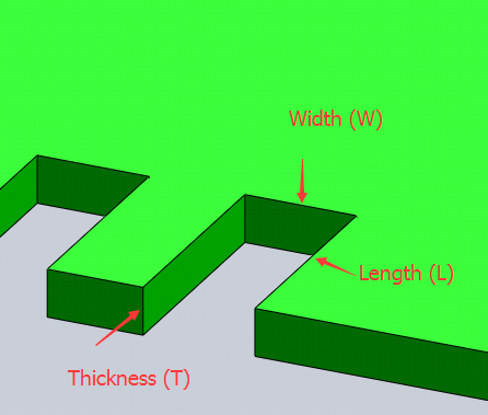
Stencil thickness calculations
The industry standard IPC7525 provides two major parameters for determining the stencil thickness and aperture size:
-
Aspect Ratio
The width of aperture / thickness = W/T
The lowest acceptable aspect ratio is 1.5.
-
Area Ratio
Surface area of aperture / surface area of the aperture walls = L x W/ (2 x (L+W) x T)
The lowest acceptable area ratio is 0.66.
However, there are are special considerations for real PCB assembly. Here are the stencil thickness design principles:
- The stencil thickness should satisfy the most fine-pitch QFPs and BGAs, while taking into account the smallest chip size.
-
When the QFP pitch ≤ 0.5mm, the sheet thickness can be selected as either 0.13mm or 0.12mm;
If the pitch> 0.5mm, then the steel thickness can be between 0.15mm - 0.20mm;
If the BGA ball pitch > 1.0mm, then select a 0.15mm thickness.
If the 0.5mm≤BGA ball pitch ≤1.0mm, then select a 0.13mm thickness.
Component Type Component Pitch (mm) Component Thickness (mm) CHIP 0201 0.12 0402 0.10 QFP/QFN 0.65 0.15 0.50 0.13 0.40 0.12 0.30 0.10 BGA 1.25 ~ 1.27 0.15 1.00 0.13 0.5 ~ 0.8 0.12 1.25 ~ 1.27 0.15 - It is a priority to select the thickness by BGA or the smallest component if two or more different ICs are simultaneously placed on the board.
- Step stencil may be applied if the thickness will be 0.1mm for matching a fine pitch component with an area ratio of 0.66, while requiring a 0.13-0.15mm thickness for other components. (Step-down) thickness should be 0.2mm for ceramic BGAs while requiring 0.15mm for other components (Step-up).
Related Articles:
Please briefly describe the information you are seeking in the search bar below.